To complement my open source BMS project I am designing an opensource waterproof Hi-Amp version of the VESC6 for use in my higher current demanding and rough for electronics electronic vehicles ( E-scooter and boat ).
I want to improve / add the following features:
Higher current capability
Add fuse to power path
Waterproof
Isolated CAN interface
EMC filter CAN interface
Rugged data and power connectors
ESD safe
Analog input filtering
I have split the hardware in two parts to keep the PCB cost low and the whole assembly “compact”. The main board that carries all power electronics will look a bit like this:
Don’t you think the total gate charge of two parallel IRF7749 MOSFETs is to much for the DRV830X? I know from calculations back in the days that with the IRFS7530 the MOSFET driver was really at its limit, when not slightly over its limit. So the Direct FETs have a lower total gate charge then the D2Pak’s from the “old VESC design”, but two in parallel result in general to a total charge higher than the IRFS7530’s.
Haven’t looked deeper in your design, but that is the first thing I noticed. Maybe it would be a good idea to use different MOSFET driver like for example rew and raphael did in their designs. That would also open the possibility to go with a higher voltage like a max of 80V or so when also the other parts are designed for that.
When I remember correctly the Toshiba TPW1R306PL looked quite good for me with a lot lower gate charge and smaller, so maybe more than two in parallel should be possible.
Thanks for responding, always nice to hear the thoughts of a colleague VESC like HW designer! The field of power electronics is so big that it is easy to overlook some limitations.
Yes, the total gate capacitance will be about 35% higher with this ESC design with respect to the VESC4.
The VESC on the old VESC the worst case total gate capacitance is 438nC (single IRFS7730), with my design I plan to implement a dual IRF7749L2 resulting in a worst case total gate capacitance of 600nC.
I think (and hope) it will work because of the following reasons: 1) I will respect the max current output of the DRV by using 10R gate resistance per FET instead of the usual 4R7. 2) I accept the higher required deadtime and the possible lower allowed switching frequency. I plan to use this ESC with low ERPM setups so that wont be an issue.
In the future I would indeed like to experiment with a different FET driver and possibly go to higher voltages, for now I first want to match the performance of the VESC6 and hopefully maybe even exceed the current specs.
Over the period of the coming couple of days I will hopefully make some serious progress to finalise the PCB design. I cant wait to get some physical experience on motor control.
This thing is looking amazing, and crazy beefy! Though im curious as to why you need so many capacitors, it seems a bit excessive lol. Also @hexakopter the TPW1R306PL looks like an amazing and cheap fet!
I’m curious too where this projekt stands. I’m already looking forward to get the BMS in my hands, so now I would love to see where the ESK projekt is going to
Yes some progress was made, but also quite a few insights where gained. First the progress!
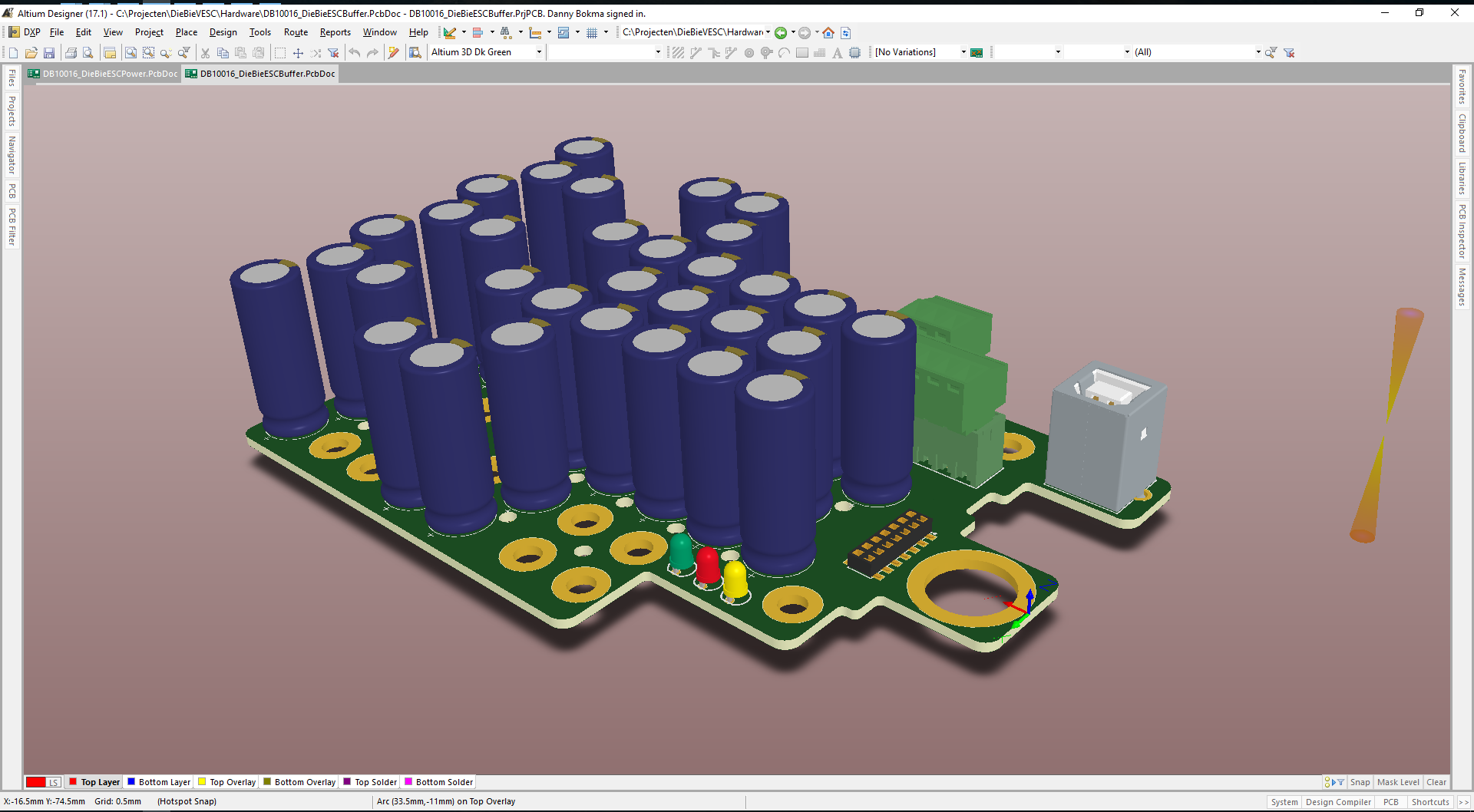
(I only made the capacitor board for now, had now big inspirations to solve the power electronics problem yet because the copper thickness I think I need are not available in the regular pcb productions).
The shown power terminals are a recent release of wurth, by pressing down on the plastic the wire terminal can be removed. They spec them up to 120A, I intent to use them for development only.
The frist images are a mocup of what I thought was the best approach to solve the cooling of the fets and shunts, I am / was still struggling with the heating of the PCB at these currents. I am still looking for a way to solve that, likely with aluminium substrate PCB’s (does anybody know a company who can make single layer aluminium substrate pcb with copper anywhere between 200um to 400um or more?).
Hey this is awesome! I had plans for a similar project. I got to the point of assembling boards but faced some issues getting it up and running and havent had the motivation (or budget) to keep going with it since.
Have you made any more progress? I would be willing to lend a hand on the design side if that will help?
On a side note, those wurth terminals are awesome, we had the rep round at work and he dropped off a few sample boards of all of their redcube terminals.


 .
. .
.

