Remembered one thing I hadn’t test yet, which was the RGB indication led on the board. Made couple short clips of it in action.

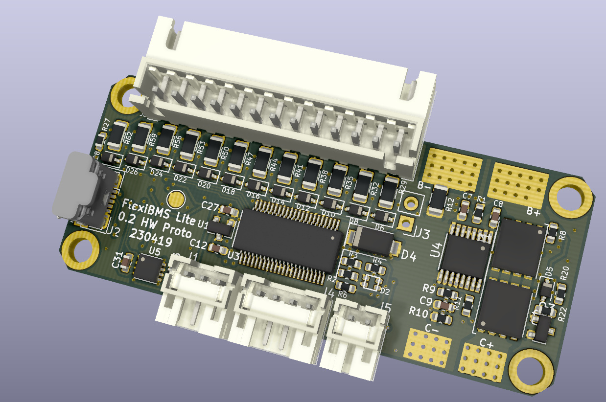
I have finished the 0.2 HW changes and I’m going to order the new PCBs this week.
Remembered one thing I hadn’t test yet, which was the RGB indication led on the board. Made couple short clips of it in action.
I have finished the 0.2 HW changes and I’m going to order the new PCBs this week.
How thick is the BMS with plugs and sockets?
I’m thinking having cables coming out both sides uses a lot of room up compared to how small the BMS is. Is it possible to raise up and spin the connectors on one side 180 deg with out the thickness exceeding 18mm (diameter of a 18560 cell) this would allow cables to be routed down 1 side layered on top of the other ones. Reducing the space you would have to dedicate to the BMS inside a build ones it’s has all its connections attached.
It’s just a idea and I have no idea if this would cause to much mechanical stress or heating issues by doing some thing like that or if it need covering with fish paper or some thing so resistors don’t melt and short cables. Or any other issue that may arise from doing that others might foresee.
Edit: This would all depend if you place you BMS next to or on top of your battery I suppose.
@SimosMCmuffin this legitimately looks amazing. The layout and design in general looks.awesome! I’m so thirsty for one of your finished products.
@Darkie02 the connectors are place like that so that there Is a battery side and a board side. All the relevant battery connectors are on one end - balance and power. And the other side is all the external inputs and outputs -can charge leads etc. Makes a lot of sense to be like this if you ask me.
Appreciated.
^This
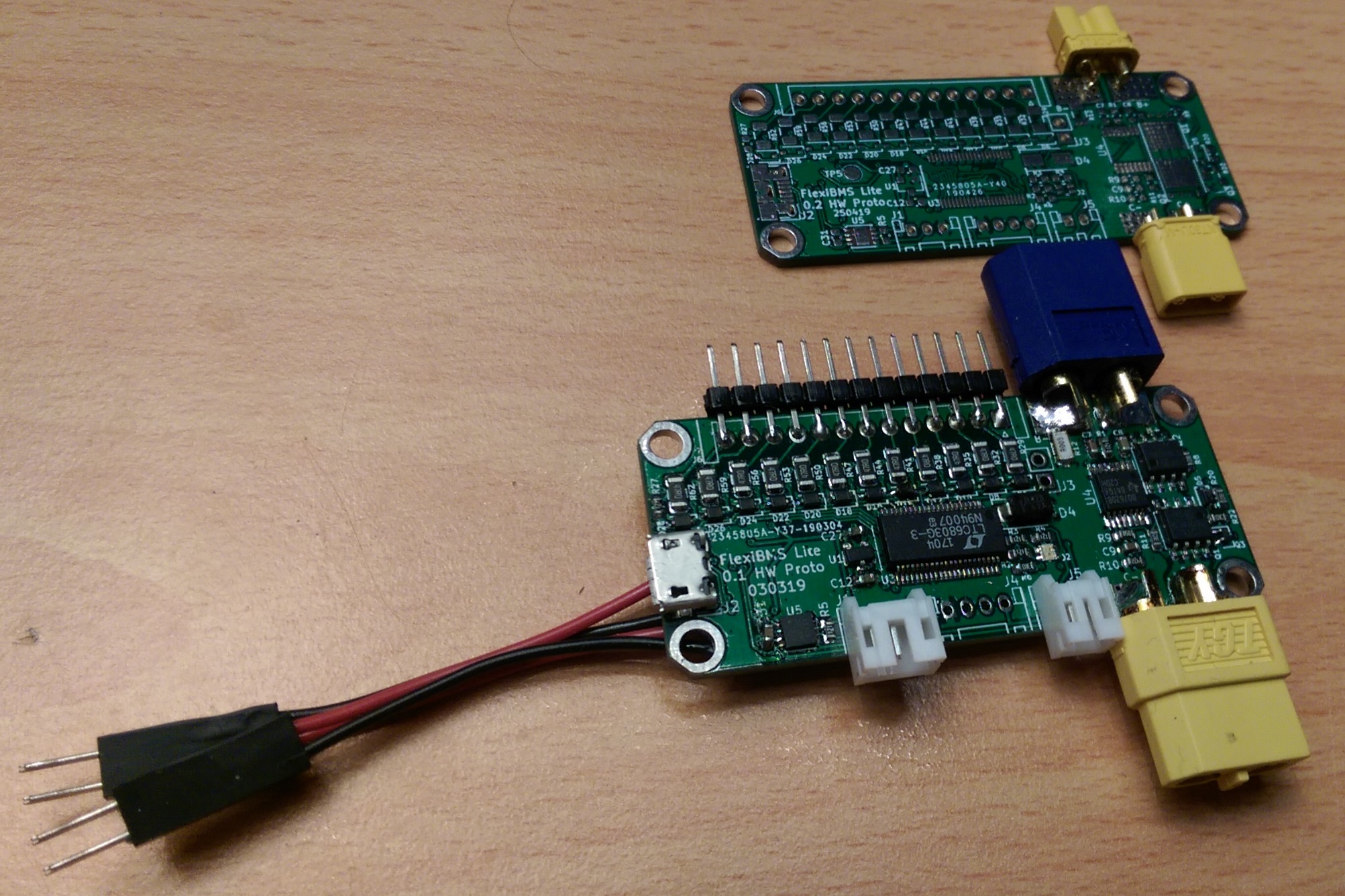
@Darkie02 The board should be under or just about 18mm thickness even if you’re using the vertical connectors and have the JST-XH balance connector plugged in with wires connected. You might need to bend the wires of on the XH quite tightly though.
If space is on super premium then you can remove connectors (or order the board without them) and solder your wires directly onto the board.
Below are top and bottom pictures of the board with the connectors named. Feel free to ask, if there is still something unclear.
EDIT: I’m gonna finish the board today and order the PCBs
As always, I love this project and has been following since the beginning of the Full version. Can’t wait to use it once it is finished.
0.2 PCBs have been ordered.
Also noticed this very interesting update email in my mailbox from Seeedstudio, I might take a further look into this.
PCBs are here. No major difference in the looks, but I also got some XT30s and I would say they are pretty ideal and just so cute next to their XT60 big brother.

I’m gonna do inventory on the components tomorrow and order what I’m missing for the next week. I think I might be able to start the assembly, but won’t be able to finish it this weekend.
This is looking great. cant wait to get my hands on one of these 
Don’t know if it would work with the lay out but I quite like these.
 https://ae01.alicdn.com/kf/HTB1ra_.KFXXXXbMXVXXq6xXFXXXY.jpg
Got the parts ordered and I’m working on the code at the moment. Cleaning up the functions and making things more clear and efficient to run.
Decided to do some destruction as a way to end the weekend.


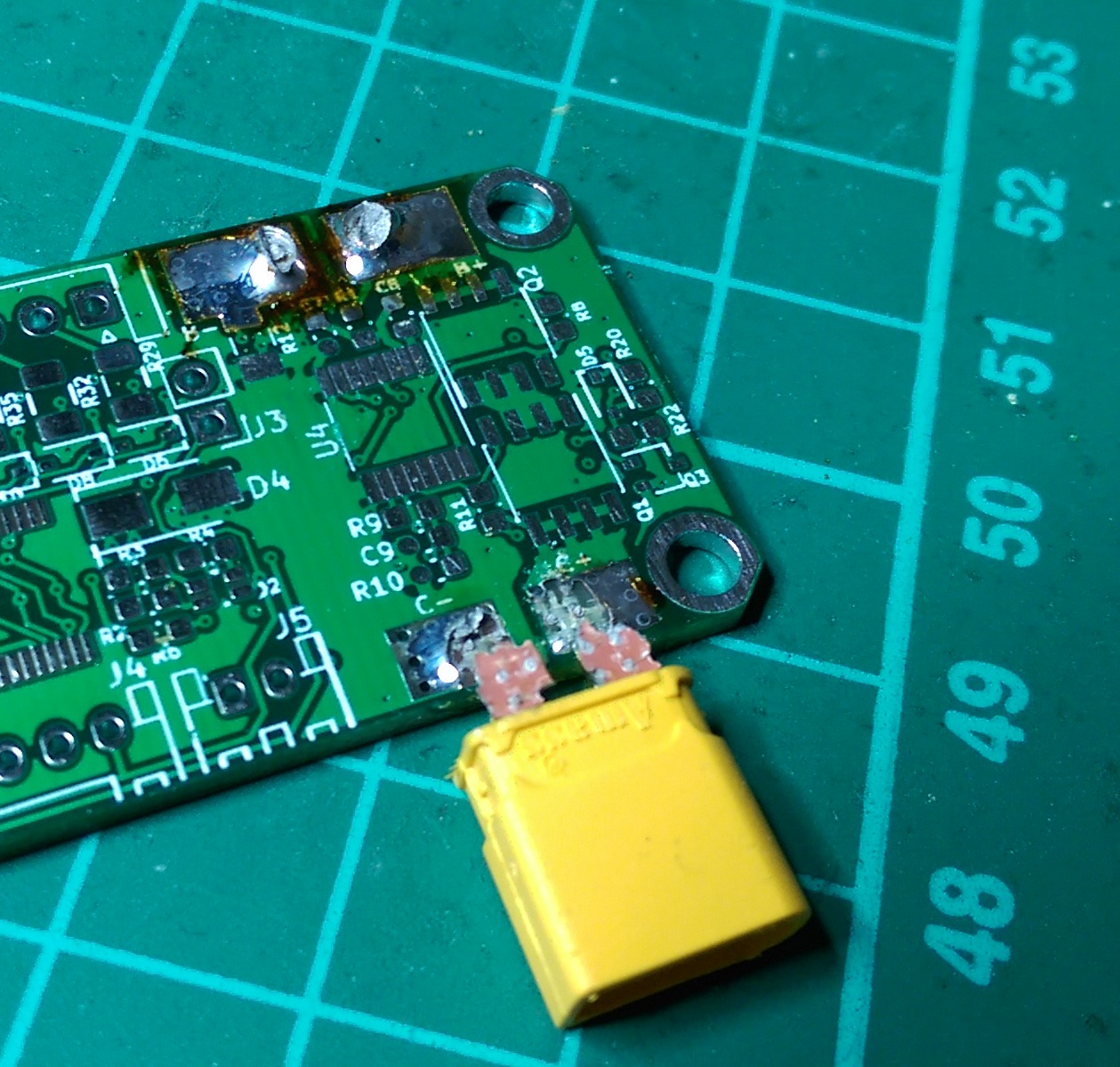
Solder joints failed on the vertical one, while the horizontal one tore the copper pads off of the board. It did take some torque to get these off. The XT30s themselves were alright and still connected nicely after this.
Note: No 0.2 PCBs were hurt in the making of these photos. Only old 0.1 boards.
Got the missing components yesterday and assembled the board this morning.


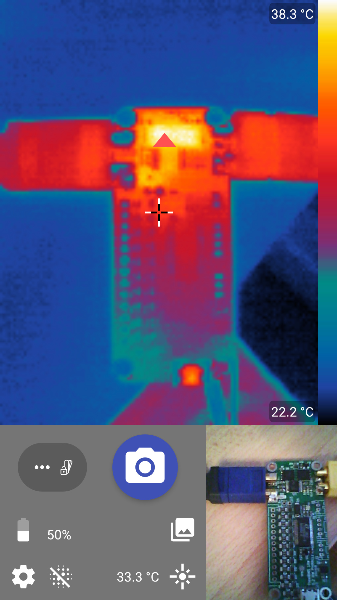
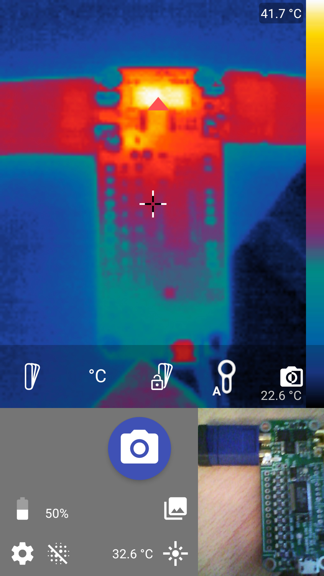
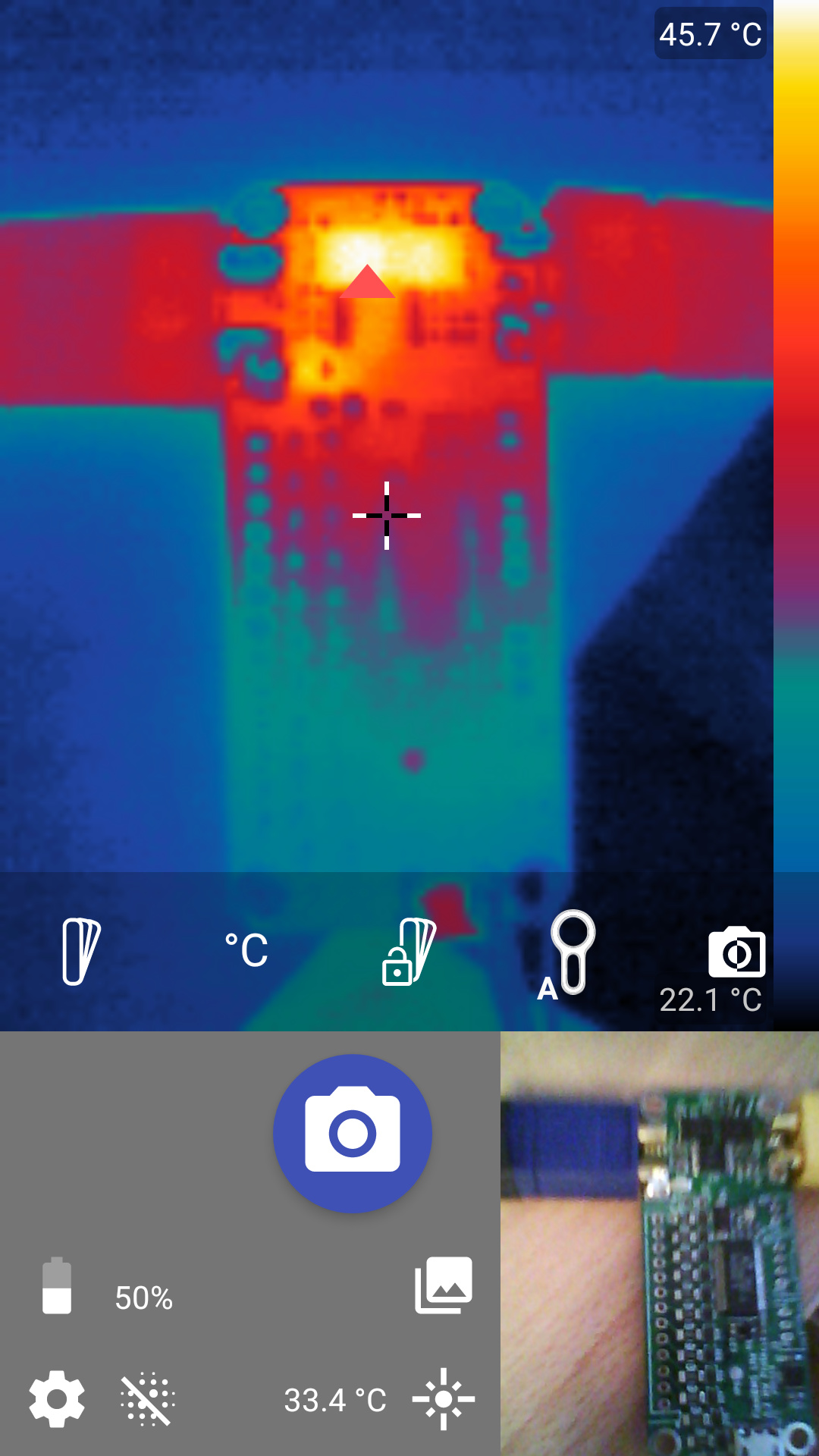
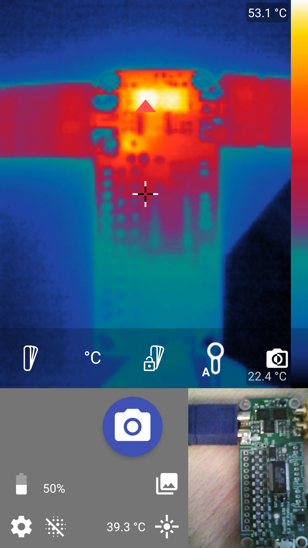
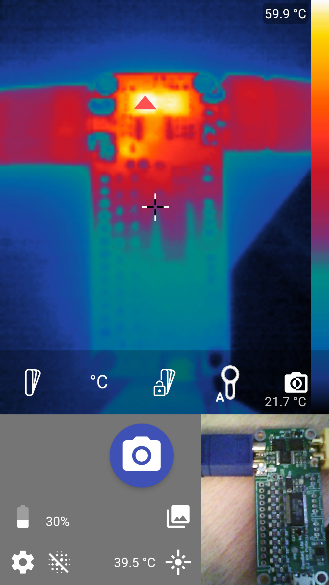
I then decided to test the max charging current. The board was allowed to thermally settle for 5 minutes before taking the FLIR images. Room ambient temperature was around 21 C. I did not measure the voltage loss over the mosfets this time, because I forgot, but the thermal images show the thermal behavior at least for the power loss in them.
6 Amps
7 Amps
8 Amps
9 Amps
10 Amps
11 Amps

With these thermal results I’m gonna say that it will do continuous 10 Amps. I also checked the current measurements from the improved current shunt sense circuit and it was within 1-2% of the indicated current from the power supply (not lab/reference grade indication), so I’m gonna say that it’s also good to go.
Any news on this project?
No big updates.
Haven’t had a lot of time to do coding, but because the hardware is starting to look fully functional I’m beginning to look into getting the prototype assembly batch under way. At least getting the real cost quotes from a couple of PCB/assembly houses and getting their feedback on the manufacturing files. I also need to think about the flashing and testing jig, so I can reduce the flashing prep & calibration steps.
Been a bit busy at work, as the customer PCB I’m doing the HW design for is supposed to be ready and sent to the fab shop for volume production next Tuesday (that’s my excuse at least) + they wanted some changes to it on Thursday. I’m also writing the most basic firmware functionality into it for this beginning milestone.
I have been also thinking and planning about how to structure the code, so that it wouldn’t start snowballing into a obfuscated mess of uncommented & confusing spaghetti monster. I’m not the most efficient or best code monkey, as I would say my skills are more on the hardware side.
I’m signing up for testing if you need any.
Seconded. Would love to aid this project in any way possible
Thanks guys.
Personally I currently see the biggest risk against getting the BMS shippable to testers being the code at the moment, but I suppose at this point as I don’t have any products to sell yet it’s just how it will be. Once I can get some additional income I can maybe start looking into getting someone dedicated for the SW side or look into other solutions.
Maybe someone from the community could help with the SW? How easy is it to flash onto the boards? If it’s easy, then as the software improves, users can easily reflash.
You can reflash with a cheap 2$ ST-link clone. In fact I use one to flash and debug.


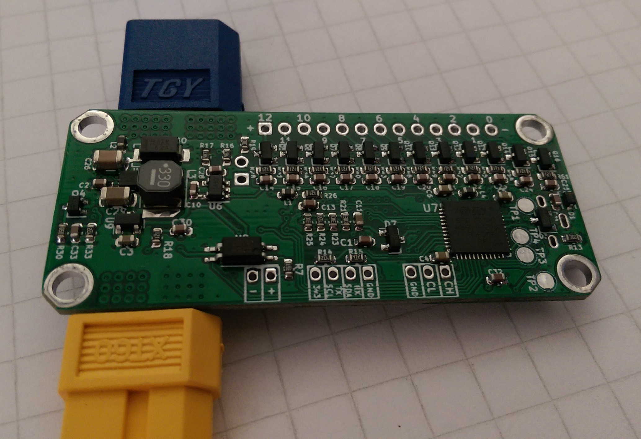
The 4 test pads on the bottom are 3V3 & GND for power and SWDIO & SWCLK for serial wire connections. Reset test pad is also available on top side (no space on bottom side). I plan on building a jig with pogo pins that I can just insert the board into and it will make the connections to the test pads for production flashing and testing. Probably gonna have pogo pins on top and bottom.
Update.
We are charging!
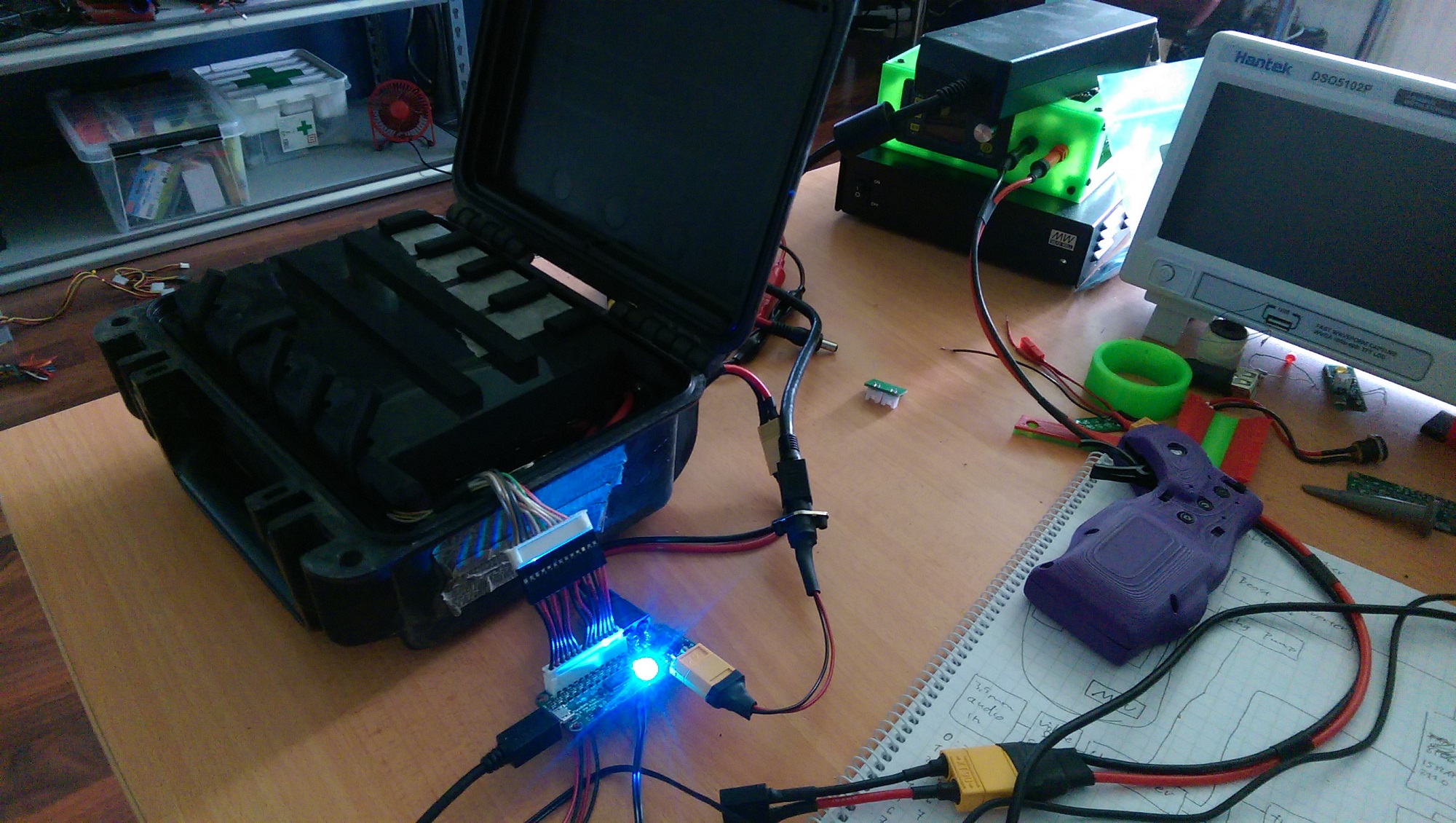
First charges going through the BMS now, got the FW sorted out so I can implement the basis for the charging control, not finished but ready for testing as I am doing atm.
I’m going to now focus on getting the prototype PCB+assembly test batch underway, alongside a debug/flashing jig, so I don’t need to use or attach the dangling debug wires onto the BMS.
On the FW side, I think I’m going to implement a communications frame for the USB-UART interface, so I can change the parameters on the fly. After this would be making the EEPROM simulation, so I can save the parameters to flash memory for non-volatile storage.

