Do you need support? Like financial?
I’m not asking for donations/money at this point in time, because that is not the current limiting factor in the development. It is time.
I work at a local engineering firm doing hardware, software and a little bit of mechanical design. I Work 8 hour days, 10 hours when you count in travel. Continuing doing the same thing when you get home is a bit rough and usually during the work days the progress is not huge every evening. Usually managing to test one specific thing. Weekends are much more productive. The pay is good, considering I graduated last year from university with bachelor’s degree in embedded systems, but I have always been active on my free time, doing interesting projects while trying to incorporate new technologies into them and develop my skill and experience through that.
Here’s a run down on how much an hardware iteration costs: 4 layer PCBs, 5-10 pcs - 38€ SMD stencils for bottom and top - 20€ Shipping PCBs and stencils - 55€ Components for a single test board ~ 70€
So I can do a whole round of iteration for around 200€, which is very cheap all things considered. The bigger loss in productivity is the turnover time for the PCBs, which is around 3 weeks, but at least now I can write firmware meanwhile I wait for the new boards to arrive.
I order my PCBs and stencils from SeeedStudio and components from Digi-key.
1 Like
I certainly hope those extra 2 hours are spent on top of an esk8. I hadn’t truly lived life until my commute was on top of an esk8. No, seriously. I thought I knew what life itself was. I didn’t.
1 Like
I wish, but Finland isn’t really the ideal esk8 country during the winter, especially with a single wheel drive (grip and torque limited) + the real possibility of turning into a human icicle. pic related.

But I’m working on a new board iteration as well. Custom deck, dual rear drive, 10S6P watertight/resistant battery pack. And I have been prioritising more ruggedness and all-terrain capability more. Here’s the raw board out of the mold. It’s shape is based on the Trampa’s HolyPro 35, but it’s made out of finnish birch veneer, which also has it’s contour limitations in the mold, AKA can’t do super tight radii, so it’s bit more rounded. It was made by one the mechanical designers at the office. You can find him @ https://www.instagram.com/pabloboards

EDIT: I think he has managed to get it cut and sanded ![]() Gonna have to make it rain on him!
Gonna have to make it rain on him!

5 Likes
How long before frank sues? Lol
3 Likes
Great work mate!
I’m in a kind of similar situation, 10-12h work per day then after reaching home keep doing same things… even for your own research, it’s quite hard 
Anyway, your mechanical designer colleague, would ship a board to Spain? My name is also Pablo and they look awesome! I will send him an email.
Found a weird glitch in the hardware while debugging the BMS and it’s making this very weird noise. I don’t know what’s causing this, so I’m just posting a short video of it in case you guys know where it might be coming from?

17 Likes
Hahaha!!! That’s definitely a weird sound dude!
Damn, rick rolled
Can this be the default power on beep?
3 Likes
em has been gotten. Noice one bro. Can you do a shooting star with it now
I like mine to have the Darth Vader theme later on 
2 Likes
Oy! I’m writing an update over here!
I’m concluding the 1000 hour pre-prototype BMS standby power use test and below is the graph produced from it. If we assume the 9mA average discharge current over the whole 1000 hours period, then it would come to 9000mAh discharged.
This will be reference to which the future discharge tests will be compared to.

As I have tested with the 0.1 HW version, it had roughly 600µA of standby current, but I have looked into the different options of lowering the consumption even more and I have couple ideas and options that I’ll try.
Hardware testing has progressed into testing the boost converter’s thermal performance. Bulk charging was also tested and temperature wise can handle 5 Amps continuous. Charging FET control needs a bit refining with resistor values, as quite a lot of heat is wasted currently.

I2C and ADC functions have been implemented and the USB driver configured, so I can read and write to/from the module via a serial terminal. SPI will need to be implemented and tested once I get the next board iteration. Below is a capture from the data stream with short explanations for the values. I can manually write the DAC values through the terminal to control the end-point voltage for the boost converter and through that control current. Balance connector is not in use due to the footprint mishap with the LTC6803-3 and the intermittent connection problem.

Here’s a thermal image of the boost converter boosting 24V up to the 10S 39.7V (at that moment) battery pack in the picture. 100W 24V 4.2A in, 96.8W 39.7V 2.44A out.

It’s running still quite hot and I’m looking at a possibility to use a synchronous boost circuit to eliminate the diode losses. I’ll probably make a standalone test board for the synchro boost circuit and test it with that.
Here’s a couple more thermal pictures of the top and bottom of the board. I didn’t note the power, but I’m assuming around 80 Watts.


With those things tested, I’m starting the planning on the 0.2 HW iteration with quite a lot to change and improve upon. I have chosen the new MCU and mapped the peripheral pins on it. I’m changing the MCU series to the STM’s L4 ultra-low power ARM, thanks to @okashira for suggesting the L4-series, which I then looked at and found to be a pretty good choice in fact.

Off-topic: Did anybody do anything interesting during easter? I bough a 12-pack of berlin donuts and ate 9 of them myself!

4 Likes
I suggest to try out STM32CubeMX for assigning pins on mcu. It also lets you choose mcu based on your needs 
1 Like
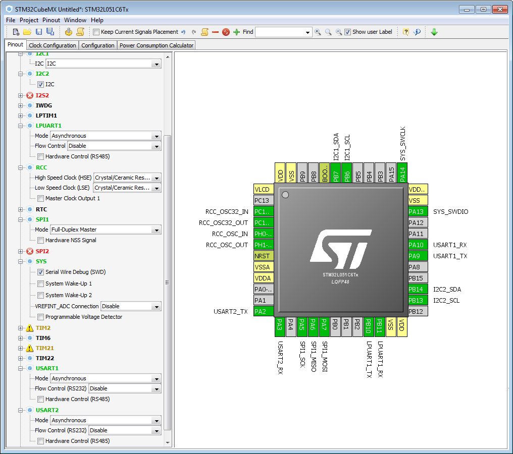
I have and do use CubeMX (have it integrated into the AC6 workbench), but I don’t like to use it to map the peripheral pins, because you can’t show all the possible peripherals for all pins at the same time, so I do it on the paper instead. I can show all the peripherals on all the pins and that helps me personally figure out faster the best combinations of which peripherals to use based on their location in relation to the other peripherals.
Nice. Glad you’re trying the L4. I think there may be a pin compatible L4 that swaps with he F3?
Yeah that’s a good point I normally map pins myself, as I don’t like auto positioning
I dont really think it would be pin compatible, but you have to check out which line and package you picking out 
Not with CAN support I don’t think? I specifically chose the L433CCT6, because it had all the needed peripherals, while still being a low pin count. + low price.
And no external oscillator needed. RTC and USB can be run with internal oscillators.
Thanks for finding that on the battman design. Not surprised there is some issue. Ultra low power design takes a lot of conscientiousness. Maybe try to increase the resistor values or if necessary, add another FET to gate it when in sleep mode.
Just a question, why you dont add diode inline of CHG fet to prevent current flowing back from the battery? Isn’t this way you will prevent current leakage?