If you don’t see a point of it then just ignore it. There are people who understand it and wants it.
1 Like
Just trying to help you think this through before you plunk down cash. What weight copper are you using, and what’s the trace width on your busses?
Let it go Let it go
1 Like

1 Like
On 20700B PCB the future is bright with possible 16S 
1 Like

Here we (almost) go https://shop.3dservisas.eu/products/18650-4-cell-pcb-holder?variant=5142975217691
Will be bit different links the minimum quantity will be 10 pcs
1 Like
Here are the links to the items. If anyone is interested in more than 50 pcs. Give a message we can make a deal then 
Well, i missed the Explanation of this PCB… what does it do?
My thoughts on these PCB’s If building a 4p the fourth battery has to stick out from PCB In order to catch the bus bar fully.and only two points of contact Even a 3p only two points on contact I wish the bus bars on pos/neg were longer so I can catch each individual battery, instead of 2


2 Likes
That pad wasn’t supposed to be used as bus bar it just solder point for connecting pad and wire together
1 Like
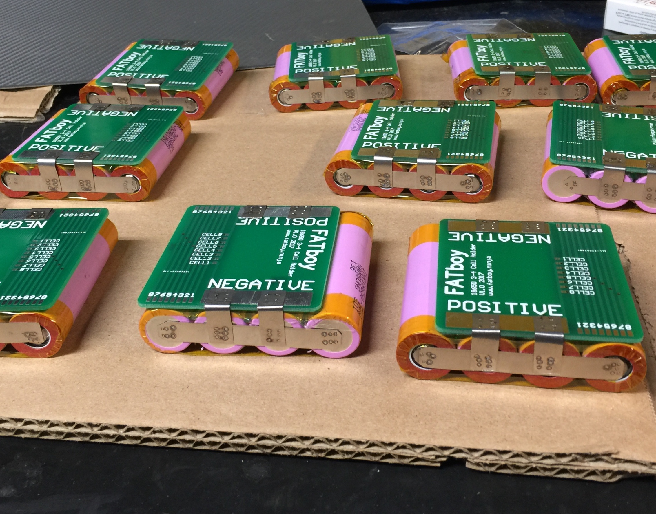
You better solder those leads to copper because I don’t think it will hold because I don’t believe they welded correctly.
Thought about that but when I tried to peel the nickel strip off couldn’t get it of easily
But still I would recommend to solder it
Ok I took your advice and put a dab of soldier on connecting nickel on tops of pcb
1 Like
@Kug3lis can you explain the balance lead jumper again on your PCB’s. I ordered some and well I think I may have asked this question when you were still designing but now that the units are out I need to ask again.
I did look at the front and back of your PCB.
See below picture… do I just fill in those two holes with solder to say for example complete the balance jumper for Cell #7? Without both those holes have a dab of solder balance cell #7 wouldn’t be indicated.

You only need to jump where the positive comes out to the bunch of pads to the corresponding one right next to it.
He has traces going on the bottom layer of the board. The holes you see are called vias and they are essentially vertical traces that connect layers on the pcb.
For the first group you need to jump cell 1 on the neg and cell 2 for the pos, for every subsequent group, you only have to jump the pos to the correct number, eg for group 2, you connect pads labeled cell 3 on the pos, for group 3, you connect pads labeled cell 4 on the pos and so on.
Ok still confused… what does jump mean. Can u put in a diagram